Milling a PCB
I’ve been making my own PCB’s for a while now. Making your own PCB’s is hard and time consuming work, my collection of failed attempts proves that. Over the last few years my process has changed multiple times, flipping between etching and milling multiple times. Milling is by far the most convenient, but etching allows for much smaller details.
My first ever PCB which used a modified 3D printer that was “printing” a one-layer tall STL file.
My history of different workflows
| year | workflow |
|---|---|
| 2021 | Etching using a mask drawn by modified 3D printer (FeCl₃) |
| 2022 | Milling using a desktop CNC machine |
| 2022 | Etching using a spraypaint mask created using a desktop laser cutter (FeCl₃) |
| 2022 | Etching using a spraypaint mask created using a desktop laser cutter (CuCl₂) |
| 2022 | Etching using a spraypaint mask created using a desktop laser cutter (H₂S₂O₈) |
| 2023 | Milling using a desktop CNC machine with autoleveling |
Etching has given me great results in the past, however, its a long process (6+ hours) that needs near constant baby sitting and I never got it to the point where it could create a PCB reliably. My latest etching process worked as follows:
Each step requires manual handling of the board and has a high risk of errors. Ofcourse a single mistake requires the whole process to start from scratch again. Milling is much easier in comparison:
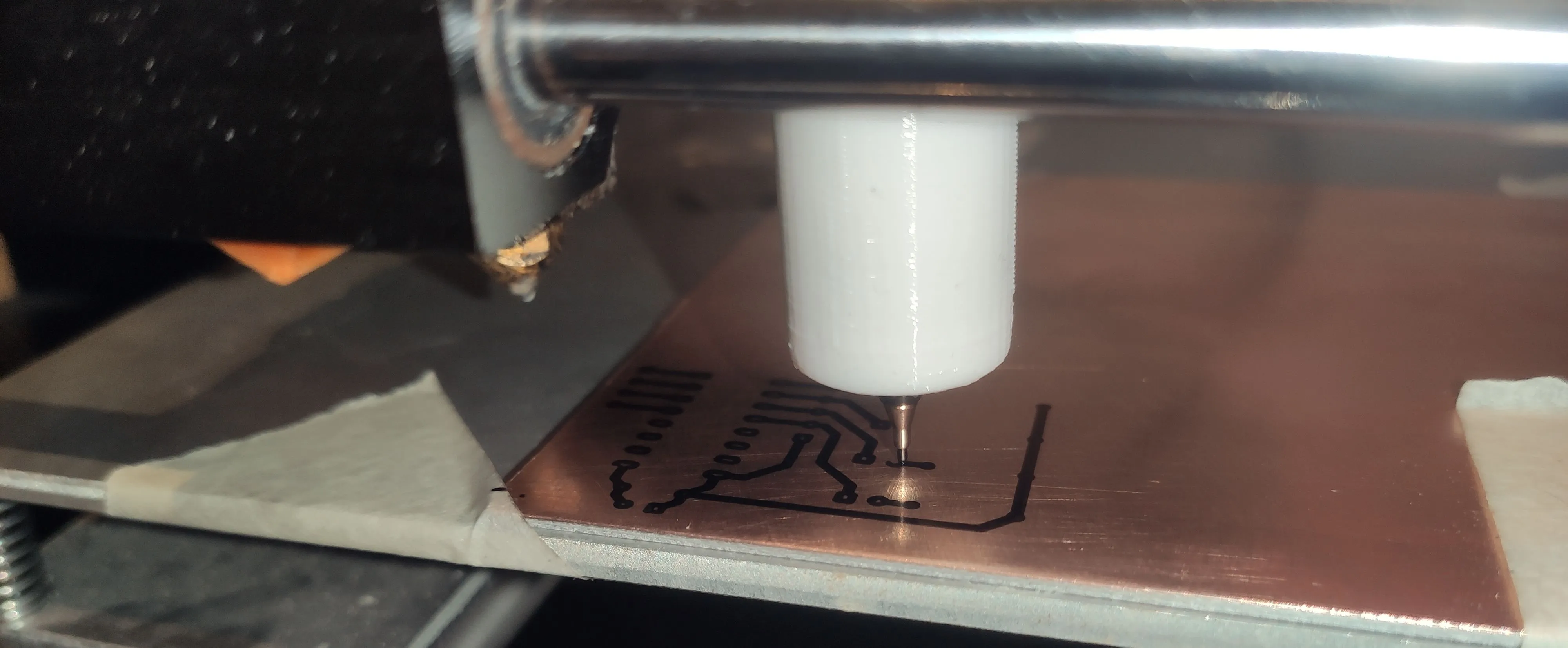
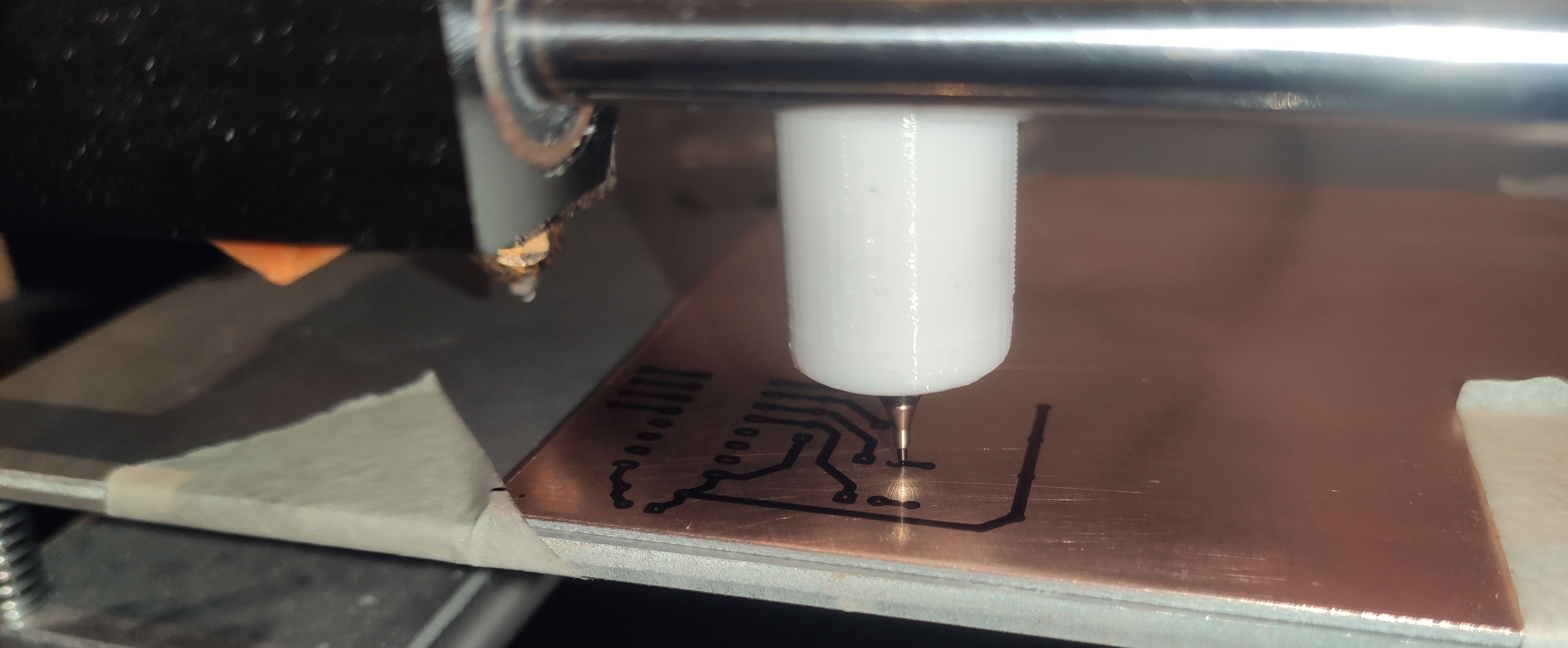
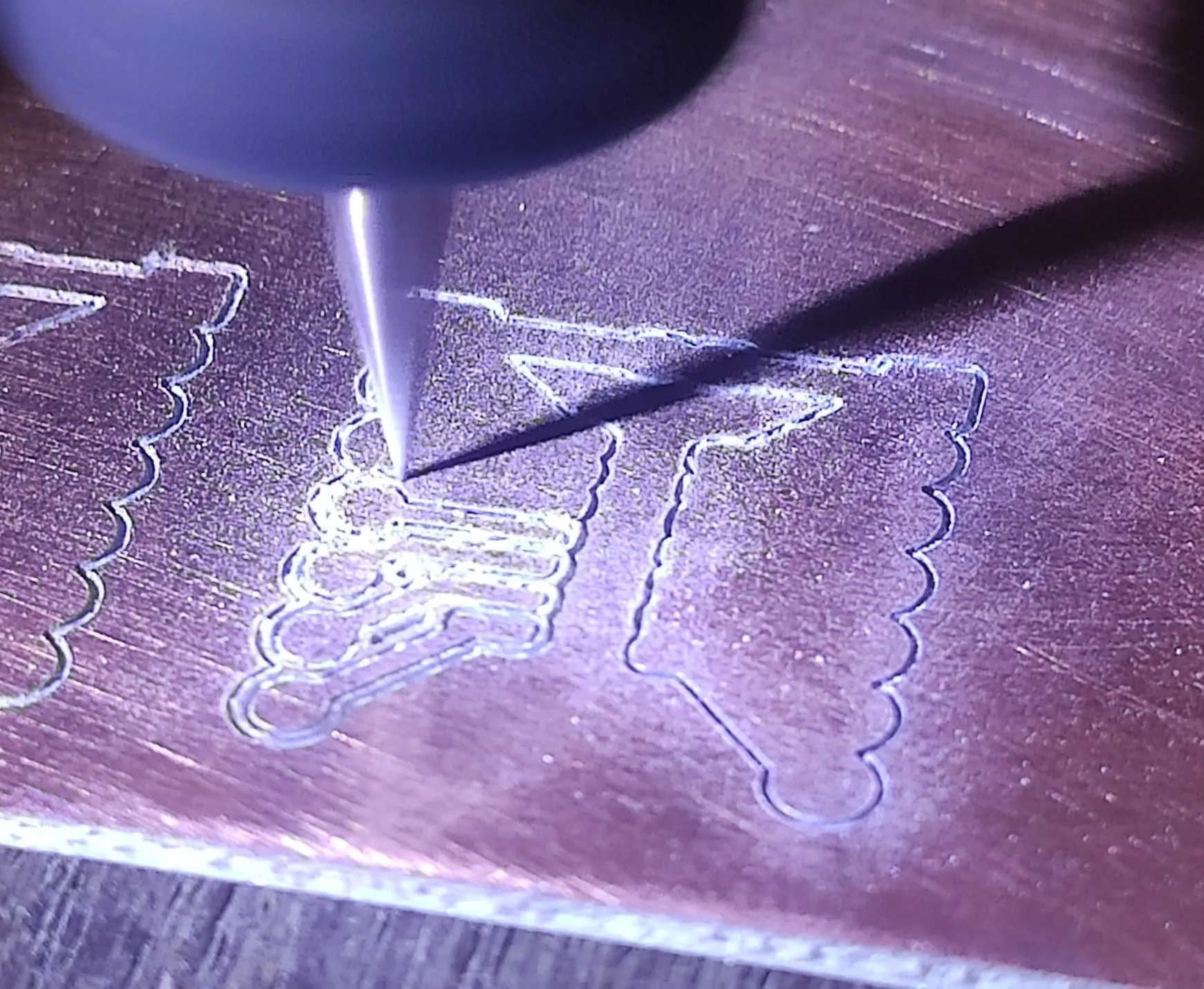
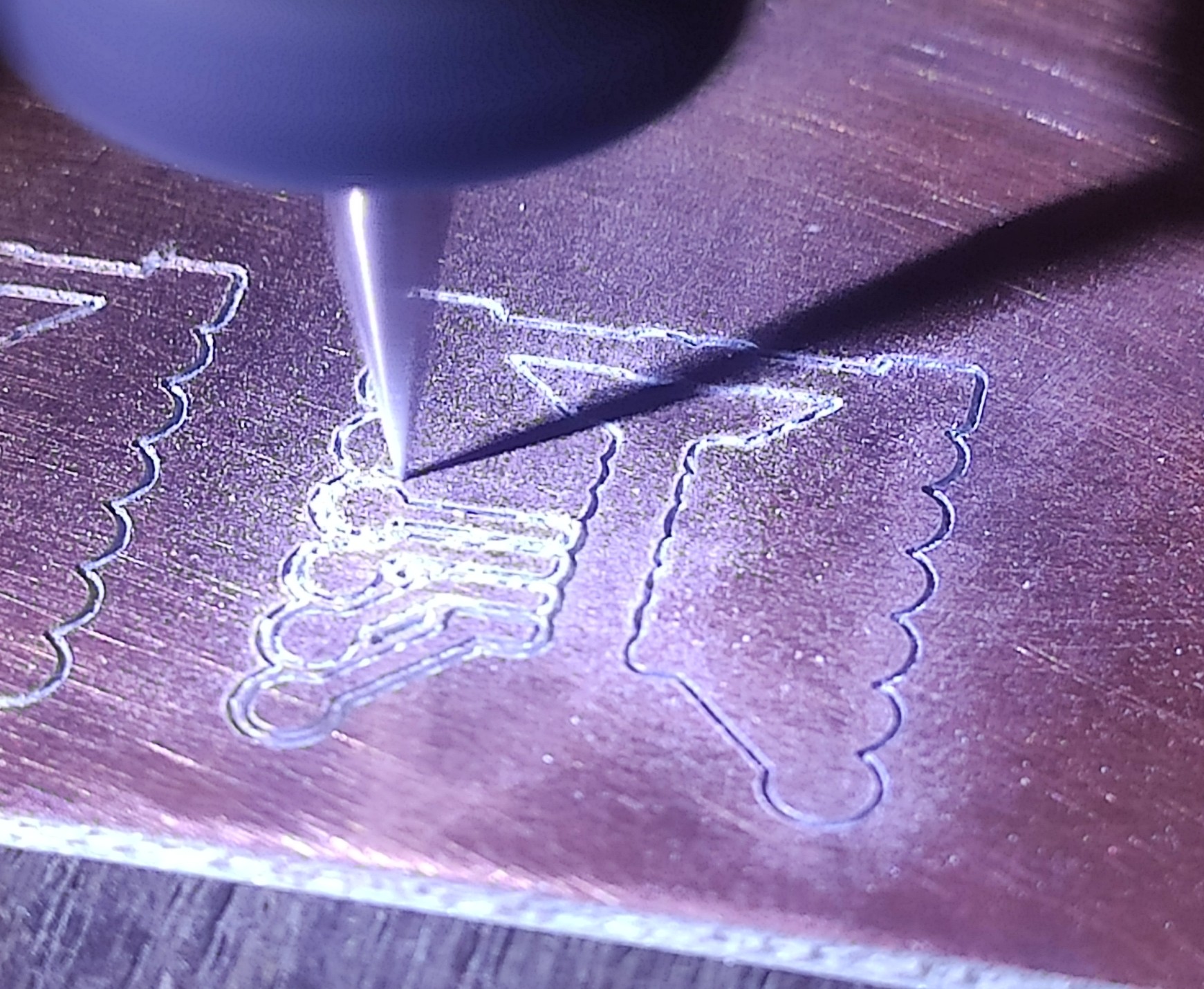
That is why milling is my preferred solution to creating a PCB. But I want to create small traces, because my designs sometimes use QFN components which have features as small as 0.2mm! The main problem with milling (on cheap desktop machines) is that thin details are difficult to create, due to the machine’s inprecision and due to the fact that a copper clad board isn’t that flat. A V-bit will have a very hard time making a consistent cut if the surface its cutting is uneven. The clad board can be warped more than a full milimetre!
Autoleveling
There is however a solution to the uneven copper surface. Copper is conductive (duh!), and we can use this property to create a heightmap. Simply connect two probes to the mill and surface, and tell bCNC to scan the surface.

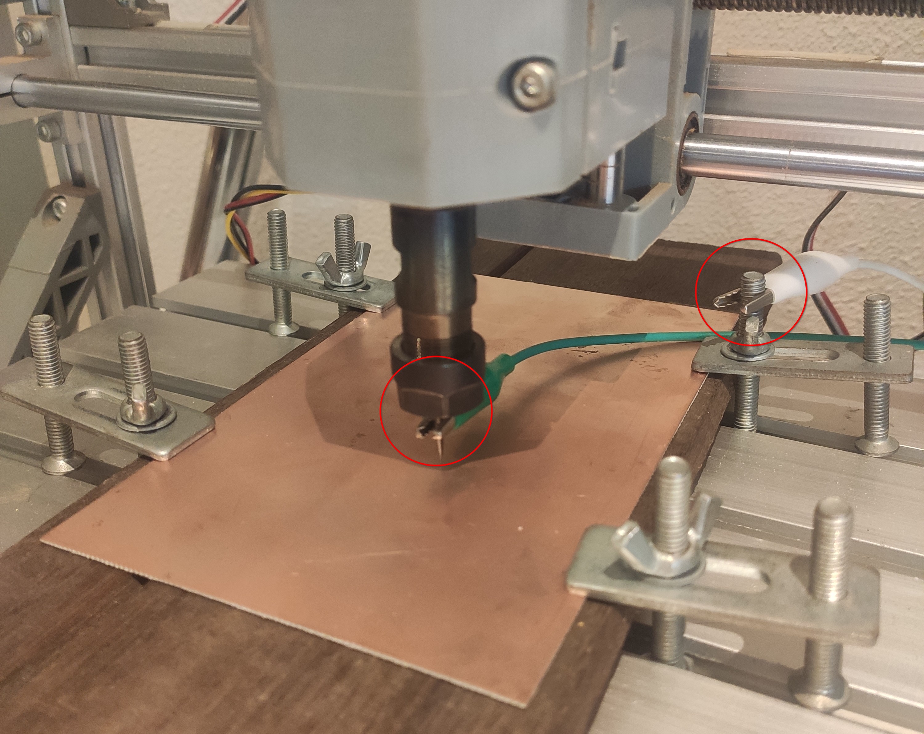

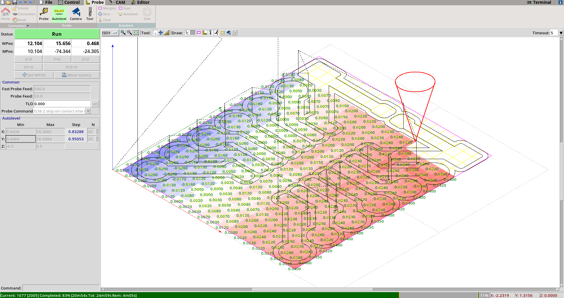
bCNC will then probe the surface in a grid, and construct an internal heightmap. It can then warp the supplied gcode using this heightmap. This ensures that the milling operation gives a reliable result with cuts of even thiccness. After this, its just a matter of finding the right depth and feedrate for your machine.

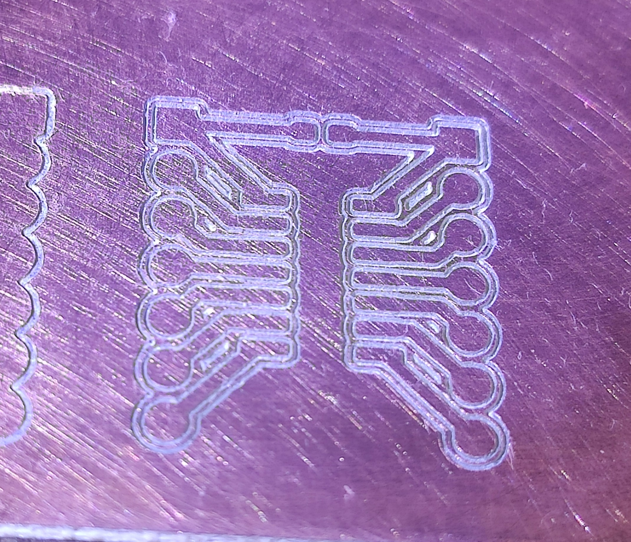
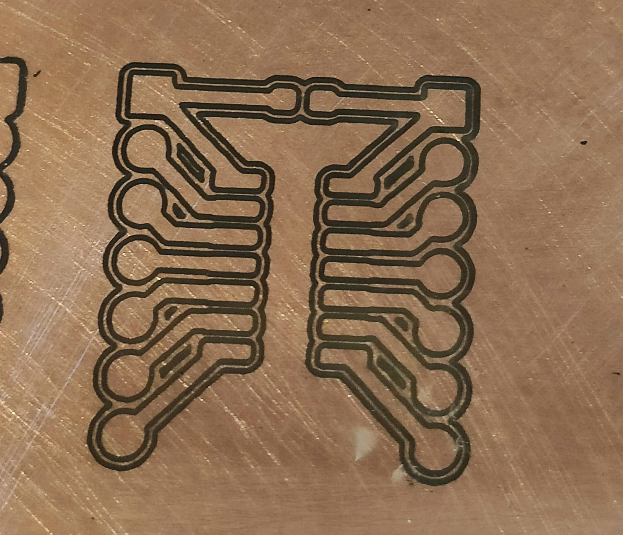
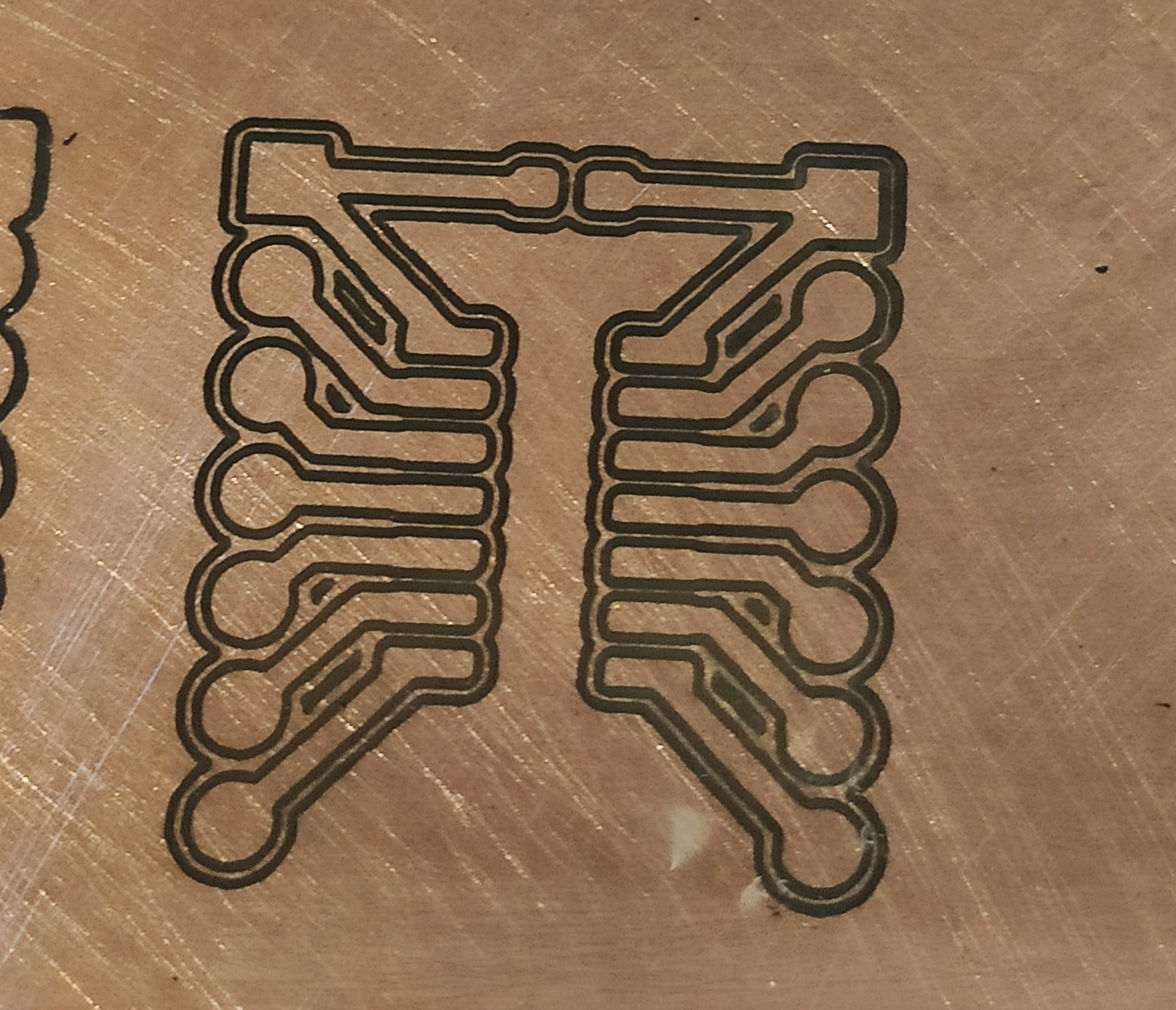
I am very happy with the result, as its comparable to etching in quality while being much easier and faster. QFN components may still prove challenging, but SOIC components are no problem.
Thank you for reading this article.If you spot any mistakes or if you would like to contact me, visit the contact page for more details.